Optical Engineering Laboratory
Optical Engineering Laboratory

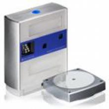
 Desktop 3D laser scanner
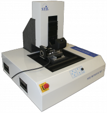
 Still Profilometer
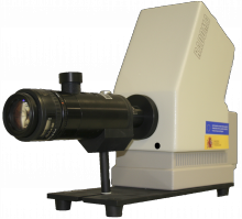
 Spectro Radiometer
 Spectro Radiometer
 Radiometer-Photometer
 Multireflection surface
The Optical Engineering Lab enables the Advanced Optics group at the Research Centre for Smart Buildings and Energy Efficiency (CeDInt-UPM) to perform its research work focused on the development of advanced optics for high field of view, high-resolution, high compactness and excellent ergonomics Virtual Reality headsets. New Photovoltaic Concentration systems that optimize cost, tolerance and conversion efficiency of conventional photovoltaic systems. Development of advanced optics for lighting systems with applications in general indoor and outdoor lighting. Optical signaling systems, automobile industry and special applications. Image-forming optics applied to improve projection systems, panoramic cameras for video-surveillance (both visible and IR) and compact telephoto lenses. Research in sub-lambda high resolution systems. Development of next generation optical sensors (for predictive maintenance of electrical networks).
More information available at: https://www.cedint.upm.es/en/research-line/advanced-optical-engineering
|
The facilities and offered techniques are assigned to the Network of Laboratories and Infrastructures of the CAM (Comunidad Autónoma de Madrid). |
|
Complete characterization of light sources
In the Optical Engineering lab we have the equipment necessary to fully characterize a light source of any type:
- Light source spectrum measurement. We have a Gamma Scientific GS 1252 spectroradiometer that allows the calculation of both the light source radiance and its spectrum from 0.25 µm to 1.1 µm, covering ultraviolet, visible and near infrared bands.
- Far-field pattern. Combined system Radiometer + Optics + Display Opsira LUCA Photometric bench, capable of measuring luminance, illuminance and luminous intensity of the source, as well as the pattern of any source of light.
- Illuminance measurement. A Gamma Scientific DR 2000-1 Light Meter/Radiometer is available for the rapid measurement of illumination without using the equipment above.
Characterization of optical properties of materials
With the available equipment one can characterize the properties as absorption, reflection and dispersion of optical surfaces and materials:
- Spectral absorption. A Newport 150w Solar Simulator 96000 xenon source is available, along with the optics needed to achieve different angular distributions of light. It is possible to know the spectral absorption of flat samples of material using this source together with the spectroradiometer.
Analysis of the quality of lenses and mirrors manufacturing
To analyze the quality of lenses and mirrors manufacturing, we have several devices that measure the characteristics of optical surfaces.
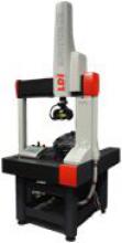
- Profile measurement. A LDI Surveyor CS 3D Laser Scanner System is available for calculating the profile of mirrors larger than 1 meter in diameter and the complete (3D) profile of lenses of any size. In addition, a NextEngine Desktop 3D Scanner is available for pieces of medium and small size, as lenses smaller than 20 cm in diameter.
- Surface roughness. Our STIL MICROMEASURE 2 3D Measuring system rugosimeter is the ideal device to analyze micro-roughness of optical surfaces that normally produce light scattering. The device can also be used to define surface profiles.
- Visualization of defects. Microscope for direct visualization of manufacturing defects on surfaces.
Measure and test of photovoltaic concentration modules
A high precision solar tracker is available to measure and test photovoltaic concentration modules.
Measure of conversion cells performance
High performance photovoltaic concentration module: pilot installation of two photovoltaic panels, each one of 12.5kW capacity, to test the long-term performance of two types of conversion cells from SpectroLab and Solar Junction.
Calibration and functional measurements of advanced optics for virtual and augmented reality systems
To analyze optics for virtual and augmented reality systems we have some devices that help us to perform functional and distortion measurements.
- Functional measurements. Imaging Source DFK 33UX174 machine vision camera + FL-BC7528-9M lens, and Westboro Photonics Smart Series USB3 CMOS P1230U Light meter + LS-10L lens to perform functional measurements, as MTF (Modulation Transfer Function), optical resolution measurement, virtual image position or focal distance measurement, that allow VR systems characterization.
- Computer controlled XYZ precision table (1 Newport CONEX-TRA25CC on each axis) for precise positioning on the three coordinate axes in order to capture different points of view through a lens and measure its distortion.
Location
The dependencies of the laboratories are located in the Centre of Energy Efficiency (Centro de Domótica Integral) in the Campus of Montegancedo.
More information HERE
Contact telephone
CeDInt concierge’s office: +34 910679600
Contact email
Scientific responsible
 |
| Juan Carlos González |
Technical responsible
 |
| Eduardo Sánchez Romero |
Projects of interest:
· For large pieces.
· Allows the scanning of objects larger than 1 meter in diameter with a precision of less than 10 µm.
· It is also capable of getting the full (3D) profile of objects of almost any size.
· Desktop 3D laser scanner for pieces of medium and small size.
· For objects smaller than 20 cm diameter it obtains the 3D profile with a precision of 1 µm.
· Surface roughness measurement.
· Up to 10nm accuracy on flat surfaces.
· Ideal device to analyze micro-roughness of optical surfaces that normally produce light scattering.
· The device can also be used to define surface profiles.
· This device allows to measure the spectrum of the light source.
· The measurable spectral band goes from 0.25µm to 1.1 µm, covering ultraviolet, visible and near infrared bands.
· This device allows not only getting the relative spectral characteristic, but, as it is also a radiometer, calculating the radiance of the light source.
· Automatic solar tracking system.
· Suitable for measuring and testing photovoltaic concentration modules.
· High tracking precision of 0.1°.